
To The Point
ETH Zurich led study demonstrates a room-temperature miniaturized Fourier-transform infrared (FTIR) spectrometer, 100 μm x 100 μm x 100 μm. A leaky waveguide scatters incoming light onto a near-infrared photoactive layer of quantum dots (QD). A gold mirror is displaced up to 100 μm relative to the monolithic device and results in a spectral resolution of 50 cm-1 (13 nm at 1,570 nm) over the range of 1 μm to 2 μm. The miniaturization of this type of sensor provides a massive potential improvement to spectral cameras, wearables, and maybe even greenhouse gas sensors.
Journal Article Source
Nature Photonics
Integrated photodetectors for compact Fourier-transform waveguide spectrometers
Abbreviations
- FTIR: Fourier-transform infrared
- PMMA: poly(methyl methacrylate)
- QD: Quantum dot
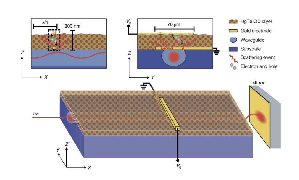
The FTIR spectrometer is demonstrated by pitching laser light (1,310 nm and 1,570 nm) into a waveguide. The waveguide is fabricated so that it leaks light and creates a scattering event at the waveguide-electrode interface. The QD layer absorbs the infrared light which leads to the measurement of a photocurrent via the electrodes. The QD layer here is what dictates the near-infrared range over which the sensor can be used. QDs can be manufactured to be photoactive at many wavelengths. The limits over which this type of sensor can be made range from 400 nm (LiNbO3 transmission limit) up to 2 μm. The 2 μm limit corresponds to the 1 – 2 μm absorbance window of the the QDs used in this study. It may be the case that QDs can be tuned to work further into the infrared spectrum.
In addition to the compactness of the sensor, the researchers in this study demonstrate a unique way of depositing a gold electrode onto a temperature-sensitive QD layer. Typically a layer of poly(methyl methacrylate) (PMMA) would be deposited and then annealed at a temperature of 180° C. QDs however oxidize and are destroyed at such high temperatures. This study demonstrates a way to create a thin floating PMMA layer through copper etching, and then “fishing” the QD layer and substrate through the liquid-air interface, thereby covering the QD layer with PMMA. This process is hard to illustrate through words alone so I recommend reading the paper and its illustrations for more details. With the PPMA layer on top of the QDs, a gold electrode can then be deposited on top of the device. The 60 nm gold was deposited using electron-beam-assisted thermal evaporation.
Opinion
One of the biggest limitations of this sensor is centered around the time it takes to make a measurement. This study displaced the gold mirror over 100 μm and took 160 minutes for a full scan. Obviously, this would be a prohibitive amount of time for some applications but not all by any means. I can see how this measurement time could be reduced by limiting the wavelength range over which the measurements are being made. For example, maybe you focus on a narrow region in the infrared. Another limitation inherent to FTIR spectrometers is the spectral resolution. For these types of systems, the spectral resolution is the inverse of twice the optical distance of the scan. While this is certainly a trade-off, it provides a lot of room for tuning the sensor design parameters to adequately target a narrow spectral region.
